Designs Done Right the First Time
We have gained our broad experience, from digital to sensitive analog, from thru hole to surface mount, while turning out accurate designs on schedule. Our customers have the confidence to certify Golden Gate Graphics for shipping artwork to point of use when manufacturing schedules are tight. Engineers tell us we are very easy to work with. Our PCB designers provide the best PCB layout services in Los Angeles along with the documentation and check plots in electronic form, GC-Prevue. GWK files (organized Gerber & Excellon data) or Adobe PDF files, at each stage of the design, so that the engineer can make improvements along the way. We are thus able to exactly duplicate the engineer’s intentions. The result is an unsurpassed speed of delivery and quality of the product.
Streamlined PCB Design = Accuracy Plus Speed
Even when doing quick turnaround design, accuracy comes first and we are your best choice for premium PCB layout designs coast-to-coast, from Los Angeles to New York. Any error on a printed circuit board can detract from your product and slow down your production. John Childers, the founder of Golden Gate Graphics, has found ways to simplify PCB design procedures and so produce fewer mistakes and faster turnarounds. He discovered techniques for systematically eliminating errors from printed circuit designs. PCB designers at Golden Gate Graphics have been trained in the policies and procedures John developed. They get your designs right the first time with very rare exceptions. And they produce at faster rates than less accurate PCB designers because those procedures are simple, which save time as well as eliminate errors. Looking for Custom PCB Design services in Los Angeles? Then we are your best option. We offer fast, accurate and reliable services. If we also help you complete and capture your schematics, so much the better as “Streamlined PCB Design” enters in at an even earlier stage than PCB layout. And all to your benefit.
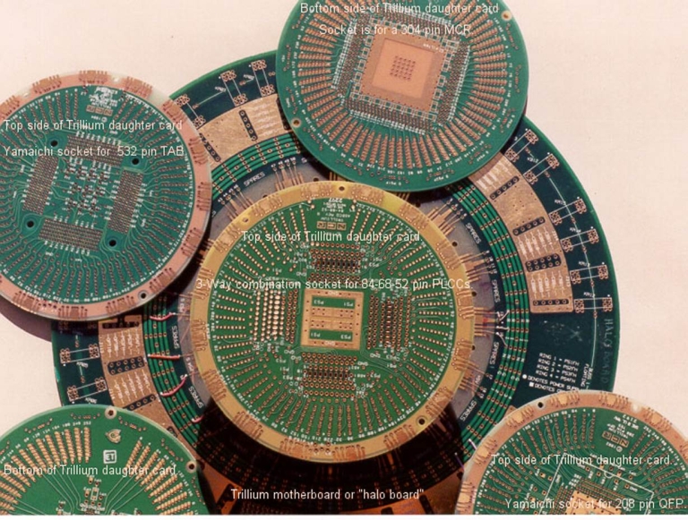
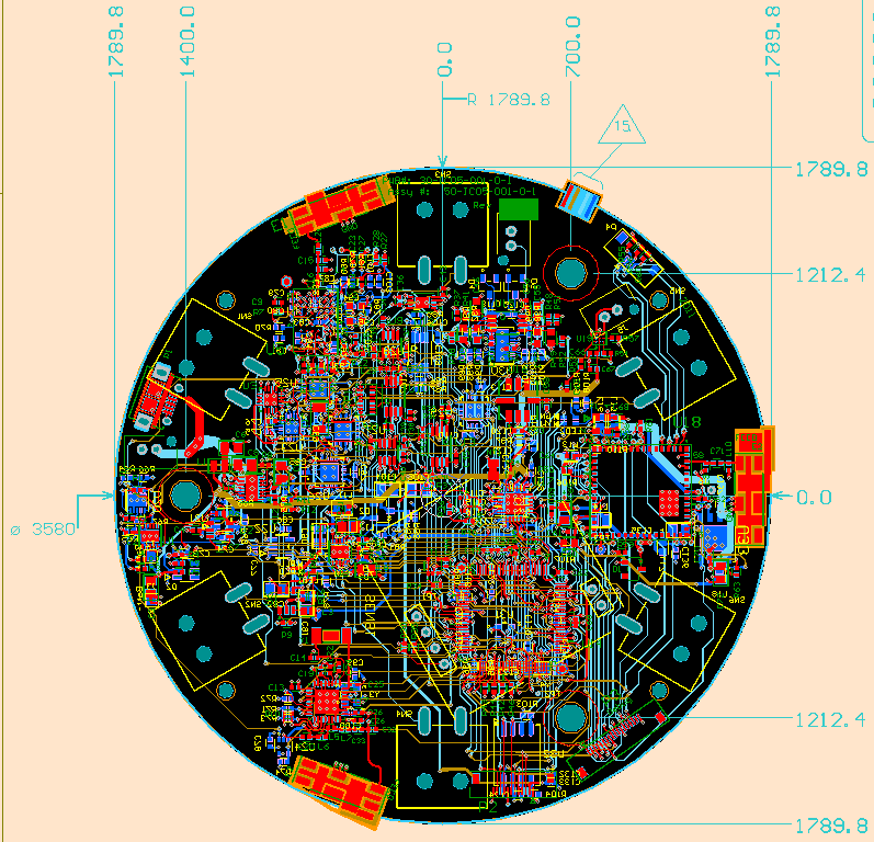
Example Printed Circuit Boards Designed by Golden Gate Graphics
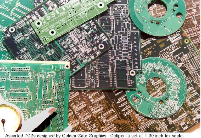
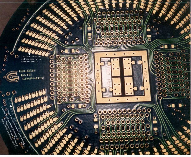
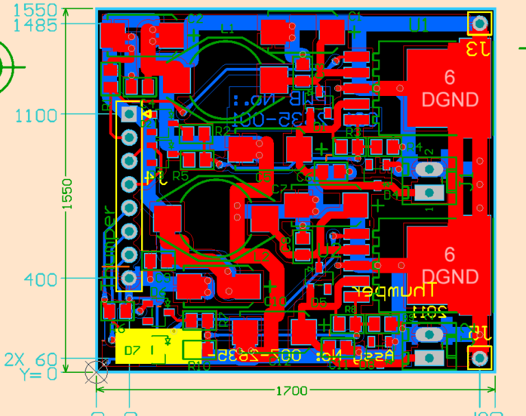
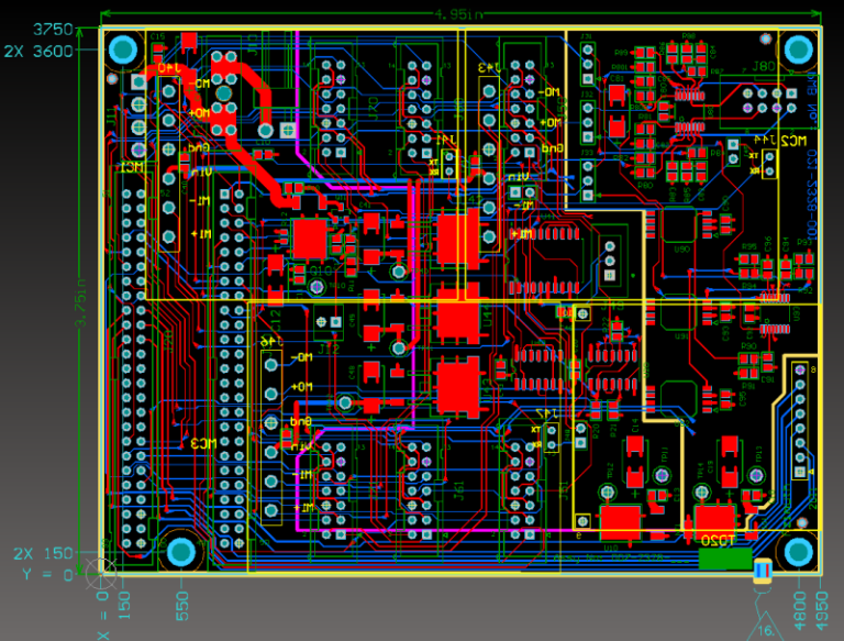
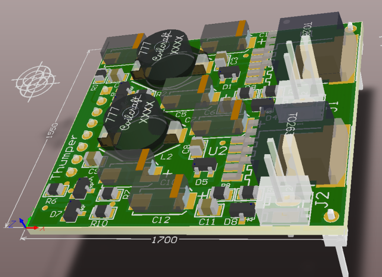
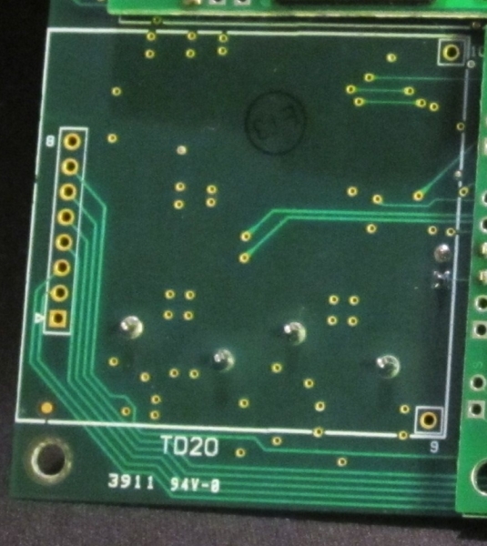
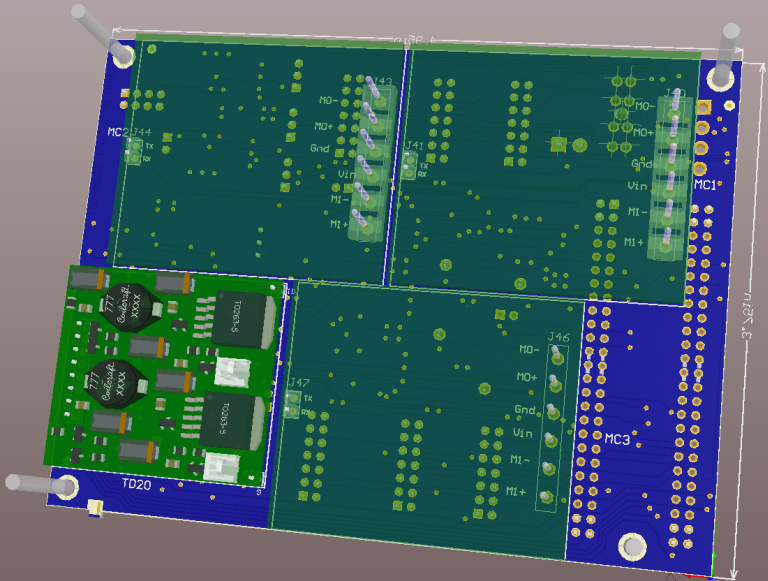
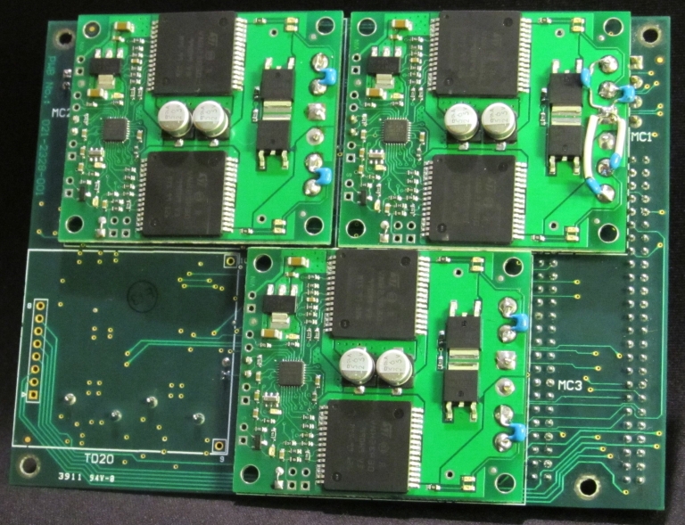
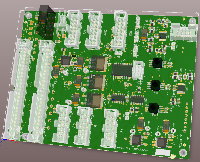
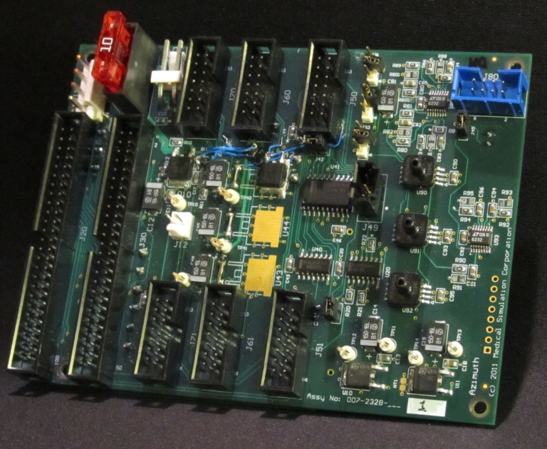
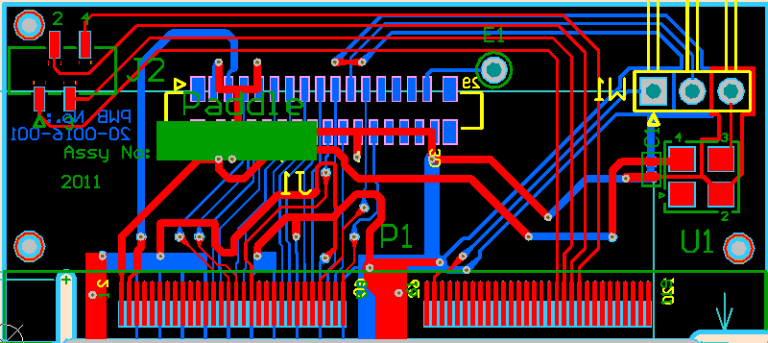
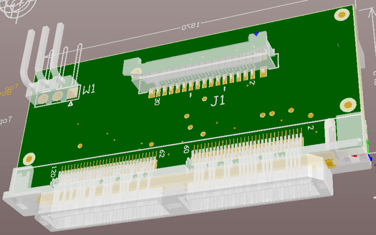
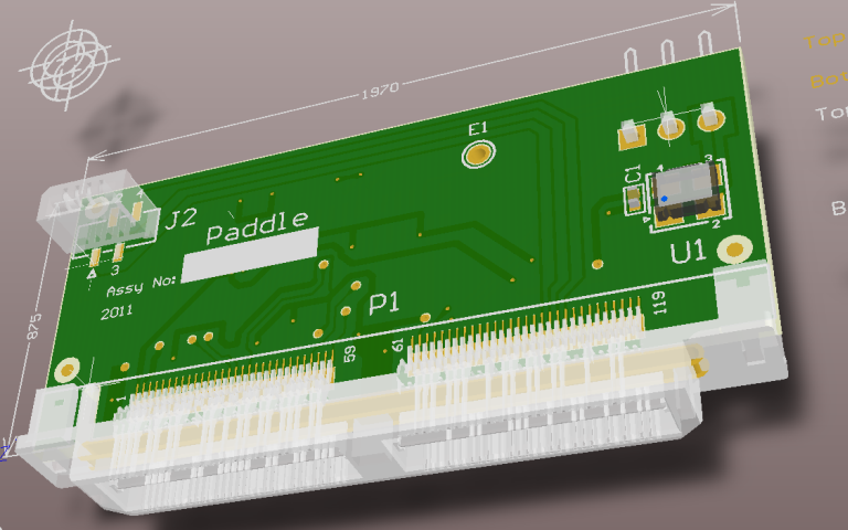
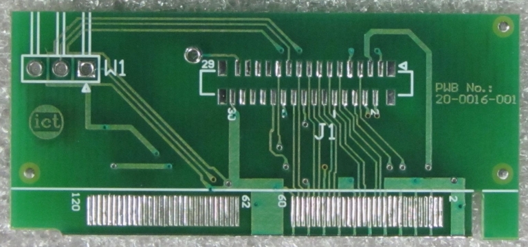
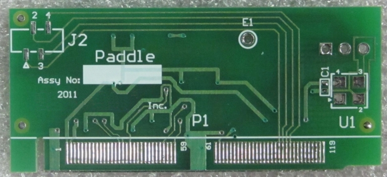
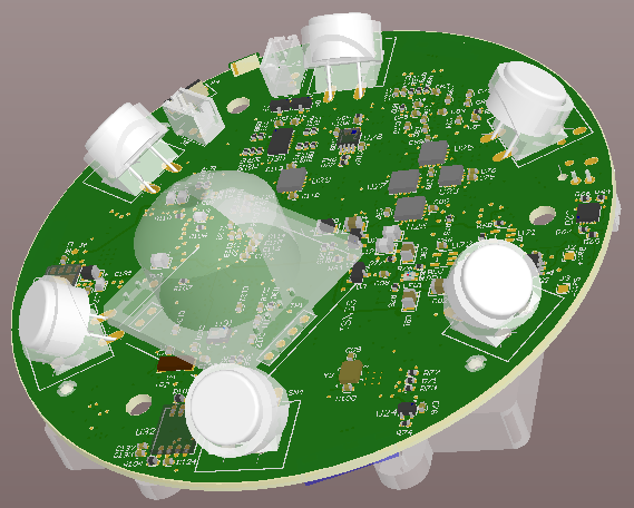
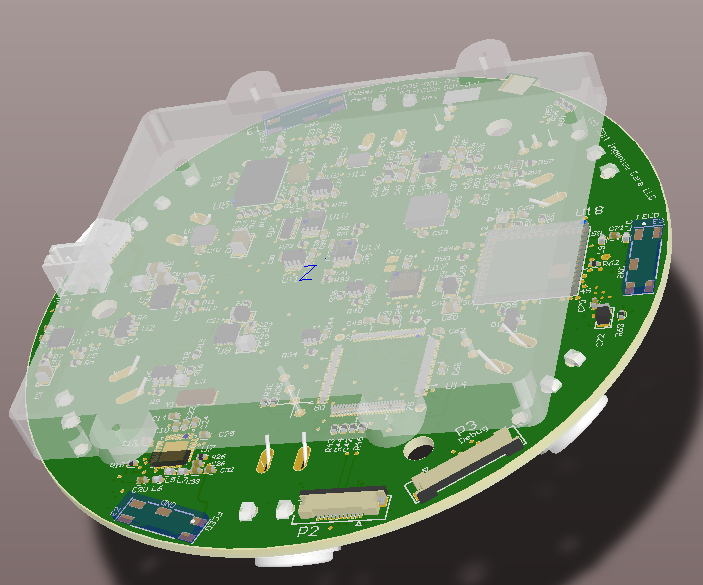
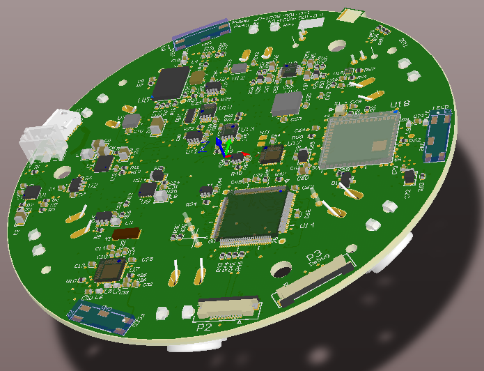
The pictures below include actual boards and design views. The 3D capabilities of Altium Designer 17, 16, 15, 14, 13 and 10 not only include the export of 3D models of the entire board, but also design rule checking of placement using both horizontal and vertical clearance constraints. To our knowledge, this is currently the only PCB design software capable of using 3D bodies in real-time clearance checking. We typically make the 3D models in our component footprints translucent so that we can see what is underneath them. Read more on techniques we use in 3D modeling to get designs to come out right.
Knowledge, Teamwork and Manufacturability
We continue to work congenially with board and assembly houses to discover their requirements and give them what they want. Our goal is for your boards to get manufactured without special editing of photo plots or use of nonstandard methods at the boarding house. This helps get your boards made faster, often ahead of schedule. Our board designs typically fly through the Engineering Department of the board house. Why? Because there is nothing to correct, and that saves you time and money. We lay out the artwork for prototypes as though they are destined for high volume production. When the circuit is working and approved for mass production, there is less design modification needed. PCB Design Service Bureau Los Angeles is known for effectively shortening your time-to-market. Put another way, we design for workability. When we help with your next electronics project design we all become part of the same team.
Ready to Talk?
DO YOU HAVE A BIG IDEA WE CAN HELP WITH?

